We are Heavy Copper PCB suppliers from China with a strong team of engineering design and technical personnel, as well as highly skilled production staff. We specialize in handling large, medium, and small batch orders. We support OME and ODM contract manufacturing, from design to PCB production. Please feel free to email us for inquiries, and we will offer you attractive prices!
Heavy Copper PCB is a printed circuit board material with excellent conductivity and mechanical strength, widely used in various electronic devices. With the continuous development of electronic technology, the application prospect of heavy copper PCB will be even broader.
All our products meet the ROHS environmental standards and other legal requirements. We have a complete system in place to ensure stable quality. Our goal is to provide top-notch service by understanding what our customers need and creating the best possible products for them.

Ion Chromatography (IC) is the industry-approved method for testing the level of ionic contamination. IC Test PCB is a important step.First, we measure the surface area of the PCB board and prepare an extraction strip. Fashion IC Test PCB .Then, we place the PCB board in the extraction strip and add solvent for extraction at a constant temperature of 80°C for 1 hour. After pre-treatment, we take the clear liquid from the extraction solution, quantify it, and test it on the IC ion chromatograph to analyze the data.Wholesale IC Test PCB.

China 20-layer PCB boards are extensively utilized in communication equipment, such as base station antennas and optical communication systems. A 20-layer PCB made in China.These devices require the processing of large volumes of data and signals. By employing a multi-layer stacking approach, 20-layer PCB boards can enhance the density and performance of circuit boards, thereby meeting the demands for high-speed transmission and large-capacity storage in these applications.

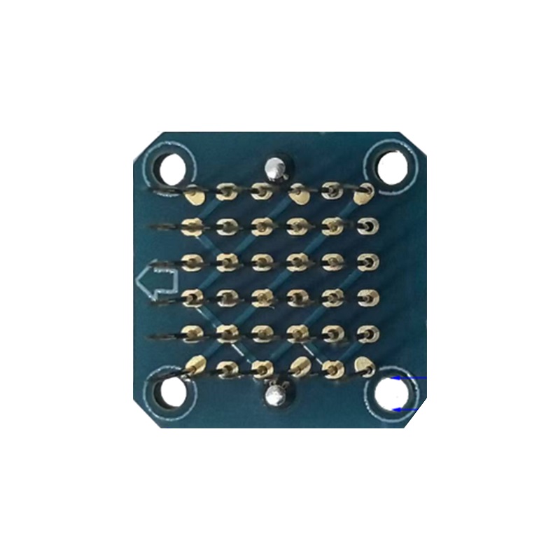
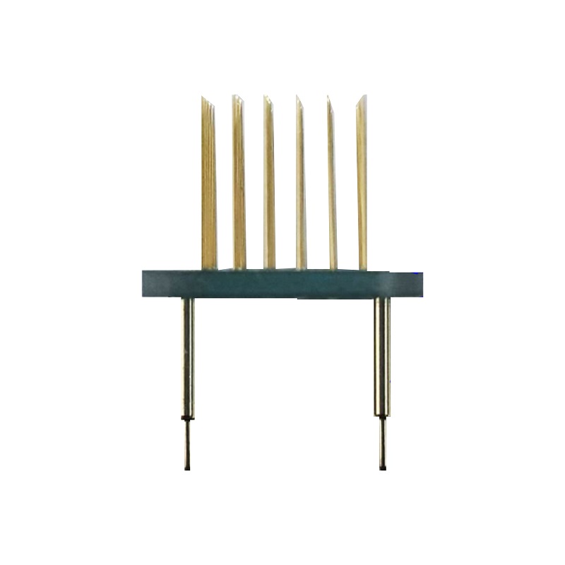
Blind Buried Hole PCB refers to the holes used to connect different levels of internal lines in multi-layer circuit boards. We are China's Blind Buried Hole PCB manufacturer. The plate does not penetrate the hole of the entire plate. The blind hole plays an important role in increasing the line density, reducing the plate size and improving the circuit performance. Blind Buried Hole PCB means that in the multi-layer circuit board, the aperture of the blind hole is welded inside the electrical connection to achieve the circuit connection inside the multi-layer circuit board.