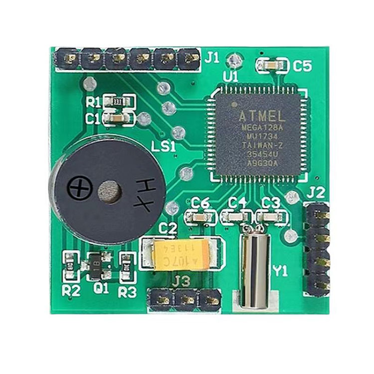

Multilayer PCB refers to multilayer circuit boards used in electrical products. Multilayer boards use more single-sided or double-sided wiring boards.
A printed circuit board with one double-sided inner layer and two single-sided outer layers or two double-sided inner layers and two single-sided outer layers is alternately connected through a positioning system and insulating adhesive materials, and the conductive patterns are interconnected according to the design requirements. The printed circuit board becomes a four-layer or six-layer printed circuit board, also known as Multilayer PCB.
With the continuous development of SMT (surface mount technology) and the continuous introduction of a new generation of SMD (surface mount devices), such as QFP, QFN, CSP, BGA (especially MBGA), electronic products have become more intelligent and miniaturized, thus promoting major reforms and progress in PCB industry technology.
Since IBM first successfully developed a high-density multilayer board (SLC) in 1991, major groups in various countries have also developed various high-density interconnect (HDI) micro-hole boards. The rapid development of these processing technologies has prompted the design of PCBs to gradually develop in the direction of multi-layer and high-density wiring.
Multilayer PCB is now widely used in the production and manufacturing of electronic products due to its flexible design, stable and reliable electrical performance and superior economic performance.