
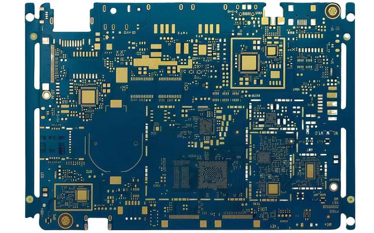
1. Introduction:
As electronic products become thinner and smaller year by year, the thickness and volume of printed circuit boards installed in these devices are smaller, which has prompted the gradual maturity of HDl technology, resulting in ultra-thin high-density HDI boards. Such boards are smaller in size, have higher hole density, and denser circuits. Similar to carrier boards, as a PCB board with a high-difficulty processing technology, it has the characteristics of ultra-thinness, miniaturization, high density, and high precision, and it also approaches the limit of PCB design and production.
2. Overview of ultra-thin high-density blind and buried hole products:
This ultra-thin high-density HDI multilayer board is made of general FR4 resin system board, prepreg, and electrolytic copper foil lamination. In the ultra-thin core board lamination, mechanical buried holes, laser drilling, and super process capacity production of core board expansion and contraction are all difficult to control. Production and processing are prone to board deformation, uncontrolled thickness, large interlayer deviation and other series of problems.
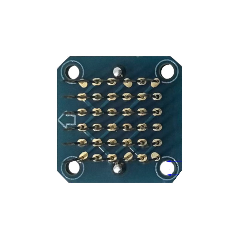
3. Product information and stacking design:
Four-layer first-order HDI (1+2+1)
Finished board thickness 0.25mm+/-0.025mm
Minimum mechanical hole 0.1mm, 282038 holes
Minimum laser hole 0.1mm, 1345698 holes (both sides)
Single size 5*5mm, number of panels 546pcs per set
4. Key control points:
4.1. Inner layer drilling
Number of holes 282038, core board thickness 0.065mm (excluding copper) After cutting, copper needs to be reduced to 7-9um, inner layer drilling minimum drill 0.1mm, customized drill bit, phenolic pad when drilling, to avoid flashing and board deformation.
4.2. Lamination:
Lamination thickness 0.22mm, single 106 P sheet, layout method 4pn/layer, control glue shortage and expansion and shrinkage.
4.3. Laser drilling:
The density of laser holes is very high, with 428241 holes on the T side and 917457 holes on the B side, with a hole diameter of 0.1mm, a single 106 PP outer layer, and an inner core board with a copper thickness of 0.065mm and 18um. The laser energy needs to be adjusted to control laser breakdown and laser hole shape.
4.4. Electroplating plug holes and surface copper:
Since the board thickness requirement is 0.25mm, the outer copper thickness does not exceed 18um, and the laser holes need to be filled with blocking points.
4.5. Solder mask:
The pad is small, and the solder mask needs to be made with LDI, and the surface treatment uses nickel-palladium-gold process.
Shenzhen Hongxinda Electronic Technology Co., Ltd. Technology R&D Center
June 18, 2021