Hongxinda Electronics is a new high-tech enterprise dedicated to the research and development and manufacturing of high-end express sample boards, standing at the forefront of industry development and breaking through the technical limits of the industry. It is highly focused on the research and development and manufacturing of high-level, high-order HDI boards, high-frequency and high-speed, and high-difficulty special process PCB circuit boards; At present, the company's monthly sample shipments are more than 100+ models and are still constantly breaking new grounds, and the delivery categories are constantly innovating.
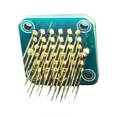
After the delivery of 7-level HDI in 2018, it successfully opened up the 4-7-level high-level arbitrary interconnection HDI market, and on this basis, it launched a high-level thick diameter (25:1) semiconductor test board in early 2019, and successfully broke through the arbitrary interconnection HDI groove board in August. This month, a buried resistor board with high transmission rate material was successfully developed.
1. Overview of high-speed material buried resistor board:
Under the current rapid development of science and technology, electronic products are constantly developing towards miniaturization, lightness, and multi-functionality. Therefore, PCB as a carrier of electronic components must also develop in the direction of miniaturization and high density. A large number of resistor components are scattered on the surface of traditional PCB boards, which occupies a large amount of board space. This seriously violates the development law of the new generation of electronic products that transmit and receive digital information at high speed, which are portable, small, light, high-performance and multifunctional. In addition, from the perspective of the reliability of PCB assembly, the stability of resistor components and electrical performance, the integration of resistor components is very necessary. At present, it is increasingly difficult to arrange and install a large number of components on the surface of printed circuit boards to meet these performance requirements. In order to continuously meet the needs of these development trends, passive components account for the majority of various electronic components generally assembled on printed circuit boards. The ratio of the number of passive components to the number of active components is (15~20):1. With the improvement of IC integration and the increase of I/O numbers, the number of passive components will continue to increase rapidly. Embedded positive technology can solve the above problems well. This technology is one of the key technologies to realize the integration of resistor components. Therefore, embedding a large number of embeddable passive components into the printed circuit board made of high-speed materials can shorten the line length between components, improve electrical characteristics, increase the effective printed circuit board packaging area, and reduce a large number of solder joints on the printed circuit board surface, thereby improving the reliability of the package and reducing costs. Therefore, embedded components are an ideal installation form and technology.
1) Forms of embedded resistors
There are many types of embedded resistor components, but there are mainly two forms: one is the embedded buried resistor technology, which is to paste various required electrical components on the inner layer of the completed circuit through SMT (surface mounting technology), and then press the inner layer with the components to bury the resistor components; the other is to print and etch special resistor materials into patterns to form the inner (outer) materials of the required resistance value, and use conventional multi-layer PCB manufacturing processes to connect with other parts of the circuit.
2) Advantages of buried resistors
The above two types of embedded resistors and etched resistors have the following common advantages over separated resistors:
(1) Improve the impedance matching of the line
(2) Shorten the signal transmission path and reduce parasitic inductance
(3) Eliminate the inductive reactance generated in the surface mounting or insertion process
(4) Reduce signal crosstalk, noise and electromagnetic interference
(5) Reduce passive components and increase the density of active component mounting
2. Introduction to the process of high-speed buried resistor board:
The buried resistor board process of the 8-layer high-transmission rate material is mainly based on the technology of embedding (embedding) resistor components, and is completed using the high-speed material of Panasonic Corporation of Japan. The main difficulty of embedding resistor components is that resistor components are easily crushed during lamination. To address this difficulty, the coefficient of variation of the resistor core board needs to be measured before lamination, and the corresponding positions of the matching PP and bare board should be pre-drilled with a drill that matches the pressed filling amine and components. During lamination, the core boards, PP, and bare boards of each layer need to be riveted to prevent layer deviation, slide plate, and exposed resistors, so as to prevent the resistors from being crushed during lamination.
Its main processing difficulties include controlling the alignment of the resistor position and preventing the components from being crushed. The single-sided structure of multiple high-speed PP plus light boards will have a series of complex processes such as slide plate layer deviation, high-speed PP resistor hole filling glue + plate hole resin plug hole saturation, small-diameter metal half-slot prone to copper exposure, hole flashing, and controlled depth back drilling.
3. Analysis of stacked structure:
The high-speed plates and PP double-pressed structures of Panasonic R5775G and R5670 used this time have impedance, holes in the plate, half holes, controlled depth drilling, L3 and L6 layer line width 0.063mm, L3 and L6 layers need to print solder mask, sink tin and paste resistors, need to drill PP and press after L3 and L6 layer chip resistors, 4 PP sheets on one side plus 1 bare board, a total of 8 PP sheets + 2 bare boards/PNL structure, hole copper 25um, board thickness 2.0mm, minimum aperture 0.15mm, aperture ratio 10.67:1 hole density 38186, surface nickel palladium gold deposition process is long, and the process structure is complex.
4. Production process:
1) Inner layer cutting - inner layer circuit - inner layer etching → inner layer A01 → transfer to 3/6 layers;
2) Lamination - glue removal - inner layer drilling - inner layer circuit - inner layer etching - inner layer AO| → solder mask - curing → tinning → testing - resistor mounting;
3) Inner layer cutting - inner layer circuit - inner layer etching - inner layer AO| → transfer to master card;
4) Inner layer cutting → inner layer drilling (GB) → - drilling (PP) → inner layer etching - transfer to master card;
5) Master card lamination 01/08 - glue removal - drilling plate hole - copper plate electricity - secondary circuit - plated hole - resin plug hole - copper reduction - copper plate electricity - secondary circuit - plated hole filling - punching (measurement of expansion and contraction - outer layer drilling - copper plate electricity - outer layer circuit - graphic electroplating - two drillings - gong half hole - outer layer etching - outer layer AOI - solder mask - character - curing - gold immersion - controlled deep drilling - Test once formed!
The 03/06 layer solder mask needs to expose the PAD of the resistor without deviation, and the surface treatment is tinning, which is convenient for mounting the resistor, and test PADs are added at both ends of the resistor to test the performance of the resistor after mounting the resistor
5. Introduction to key process technologies:
1) According to the board changes after 03/06 resistors are mounted, the actual size of the resistors and the filling requirements, determine the corresponding coefficients and the pre-drilled hole diameter of the resistor layer PP, adopt the board structure of the second outer layer PP + bare board resistor position without drilling + PP (resistor position drilling), and use high-speed PP, board and high TG material mixed pressing characteristics for one-time pressing, confirm reasonable pressing high-speed material parameters, prevent the resistor from being damaged and scrapped due to problems such as layer deviation, sliding plate, filling, and delamination caused by heat changes of the material board, and the board with the resistor cannot be over-browned.
2) Because the inner layer has been soldered before mounting, it is necessary to perform solder mask window processing on the effective board edge of the PCS unit to prevent the risk of delamination of the printed solder mask oil layer after the heat treatment of the post-process.
3) Therefore, the pre-drilled PP hole filling on the board has a certain impact on the flatness of the board surface. At the same time, the customer has strict requirements for resin plugging holes and does not allow depressions. It is necessary to adjust the height of the two plugs when plugging the holes with resin, adjust the pressure and speed to a certain extent, and then fill the holes with plating after plugging.
4) There are small-diameter metal half holes after the drawing. When the board is assembled, the board design needs to be carried out in the same direction. When drilling the half holes, a matching coefficient of the gong belt needs to be used. The tool hole of the dry film sealing hole is used for positioning to reduce the deviation of the board hole causing the half hole to be offset. At the same time, a small knife is used to pre-drill + adjust the compensation back and forth to add gong to prevent half-hole deviation, copper foil rewinding and inability to etch, causing plugging, short circuit and other problems.
5) When controlling the depth of drilling after drilling the half hole, start from the bottom layer. It is necessary to control the depth and not drill to the L3 layer. When testing, the test machine needs to be adjusted to set the resistance value before testing. Other processes are produced normally.
6. Summary:
The electronic industry is developing rapidly with each passing day. People's demand for small, lightweight, thin, highly integrated and highly reliable electronic products is increasing. Passive device embedding technology will become one of the important core competitiveness of printed circuit board companies. Through the improvement and innovation of the original process technology, it has evolved into a new process technology, which has excellent applicability and promotion value. The development of the PCB industry is a coexistence of opportunities and challenges. Only through accumulation can there be breakthroughs, meet the growing market demand, and win more market opportunities.
Shenzhen Hongxinda Electronic Technology Co., Ltd. Technology R&D Center
April 18, 2019