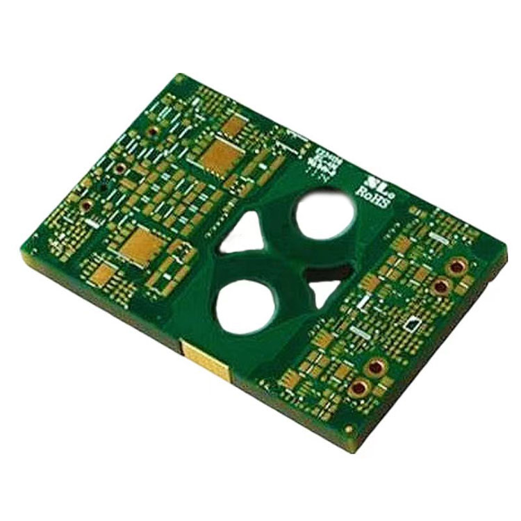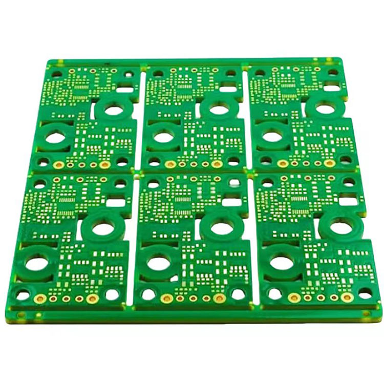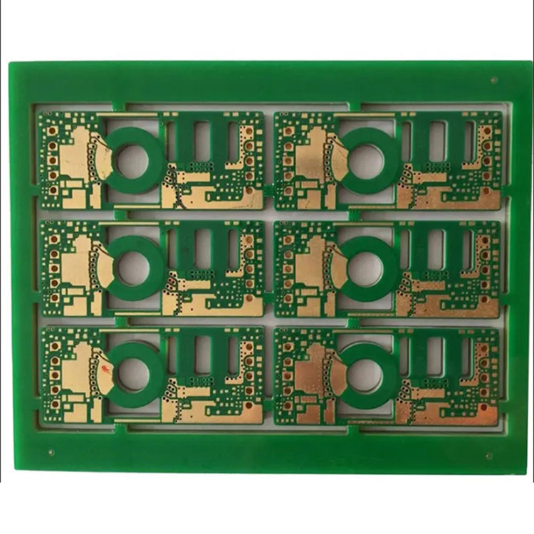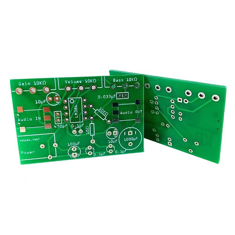
Super Thick PCB made in China can be offered for you at low price from our factory. Welcome to buy Super Thick PCB and wholesale high quality and newest Super Thick PCB Thick copper and ultra thick PCB have high current carrying capacity. In PCB boards, copper layers are used to connect different circuit components and carry current. When the circuit board needs to carry a large current, a thicker copper layer needs to be selected. Generally speaking, the copper layer thickness of thick copper ultra thick PCBs is between 2oz-20oz. This type of PCB board can carry a large current and ensure the stability and reliability of the circuit board.
We are a china Super Thick PCB factory,thick copper plate PCB is a type of printed circuit board (PCB) that is bonded with a layer of copper foil on its glass epoxy substrate. When the thickness of the copper foil is greater than or equal to 2 ounces (i.e. ≥ 2 oz), it is called a thick copper plate PCB. Copper achieves conductivity on circuit boards, while thick copper PCBs have the characteristics of carrying large currents, reducing thermal strain, and good heat dissipation.
Items Feature:
Layers: 2
Base Material: FR4
Board Thickness: 3.2 MM
Copper Thickness: 35 um
Soldermask: Green
Idents: White
Finishing: Hot Air Soldering Level (Lead Free)
Super Thick PCB Fabric Capacity:
NO Item Craft Capacity
1. Layer 1-28 Layers
2. Base Material for PCB FR4, CEM-1, Aluminium, High Tg MaterialHigh FrequenceROGERS, TEFLON, TACONIC, ARLON) Halogen-free Material
3. Rang of finish baords Thickness 0.21-7.0mm
4. Max size of finish board 900MM*900MM
5. Minimum Linewidth 3mil
6. Minimum Line space 3mil
7. Min space between pad to pad 3mil
8. Minimum hole diameter 0.10 mm
9. Min bonding pad diameter 10mil
10. Max proportion of drilling hole and board thickness 1: 12.5
11. Minimum linewidth of Idents 4mil
12. Min Height of Idents 25mil
13. Finishing Treatment HASL (Tin-Lead Free), ENIG(Immersion Gold), Immersion Silver, Gold Plating (Flash Gold), OSP, etc.


