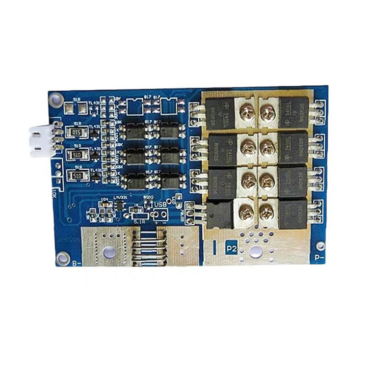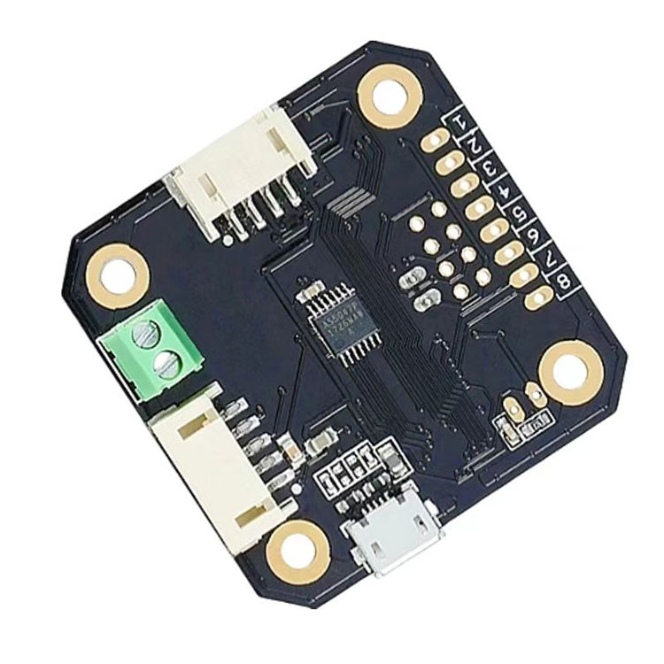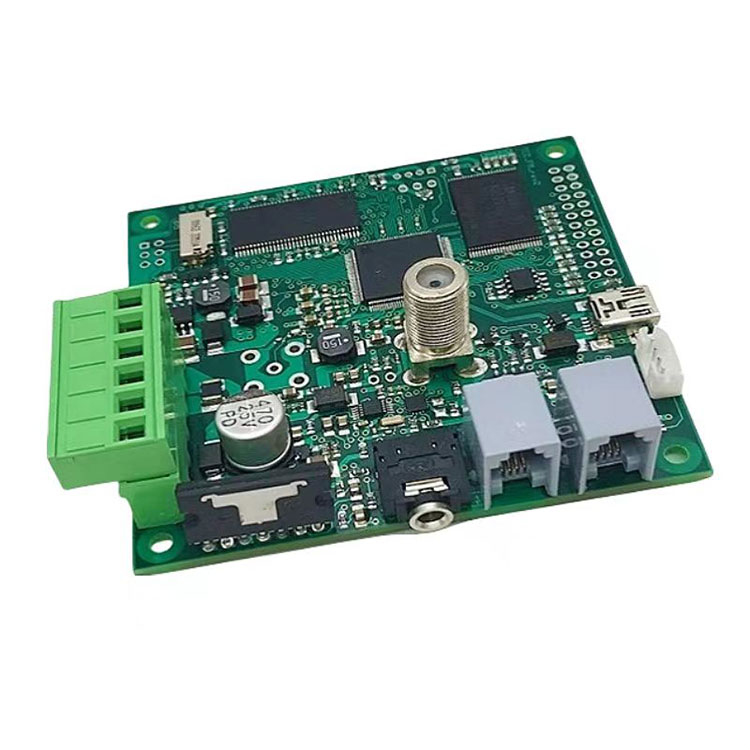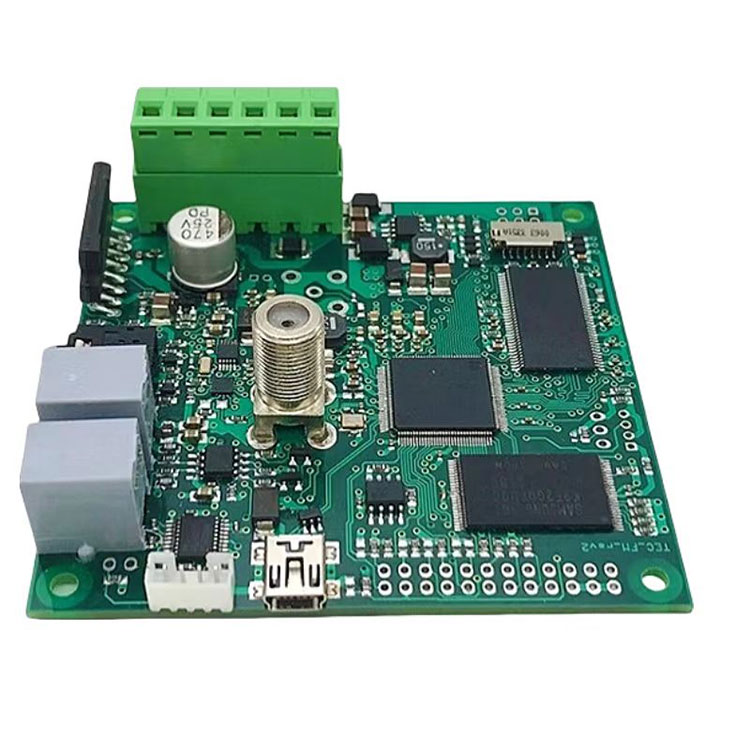
Wholesale 7 Layers PCB Board is a more advanced type of multilayer board. This board comprises 7 copper layers. These 7 Layers PCB Board include power planes, ground planes, and routing layers. Customized 7 Layers PCB Board is ideal for high-speed applications since they include more routing layers.
A 7 Layers PCB Board manufacturers use copper-plated holes to interconnect all the layers in this PCB. A 7 Layers PCB Board is complex by design. The top and bottom layers appear as dual PCB. However, there are stacked layers on the two sides of the core. Manufacturers compress all the layers to create a 7 Layers PCB Board.China 7 Layers PCB Board, manufacturers assemble the active and passive components on top and bottom layers. The inner layers are for routing. Furthermore, a 7 layer PCB has a top layer, inner layers, and a bottom layer. The thickness of a multilayer board increases as the number of layers increases.
Basic information:
Item name: 7 Layers PCB Board
Customized: Customized
Material: Fr4, Al
Test100% E-Test
Application: Electronics Device
Surface Finishing: HASL, Immersion Gold, OSP
Specification: PCB Assembly and PCBA assembly
Origin: China
Production Capacity: 50000PCS Each Month
Base Material: FR-4
Copper Thickness1-6oz
One Stop Service: PCB Assembly, Component Sourcing, Box Building
Design Rules for a 7 Layers PCB Board:
Route high-speed signals on intermediated layers. Ground planes can protect and tolerate the radiation coming from the tracks.
Ensure you place signal layers very close to each other.
It is better to use more ground plane boards since they enable signal routing
The mass and power planes must couple rigorously.
Ensure the insulation between a signal layer and adjacent plane is thinner.
Use multiple ground planes. They reduce the ground impedance of a board. Also, they minimize radiation.
Make use of efficient software to design stackup.
Consider the thickness of every signal layer.


