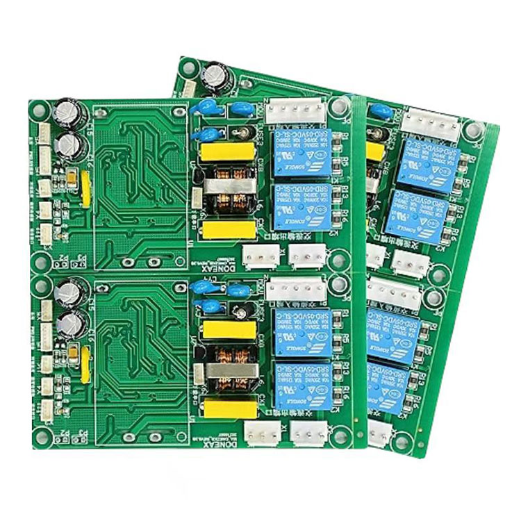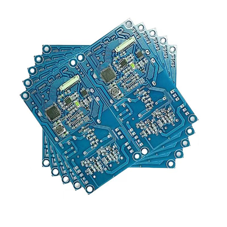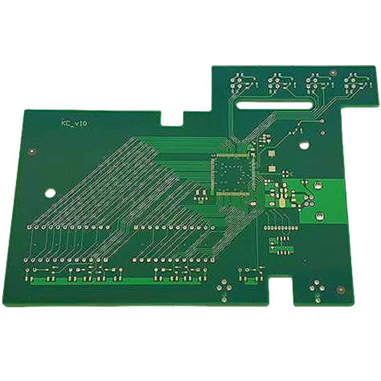


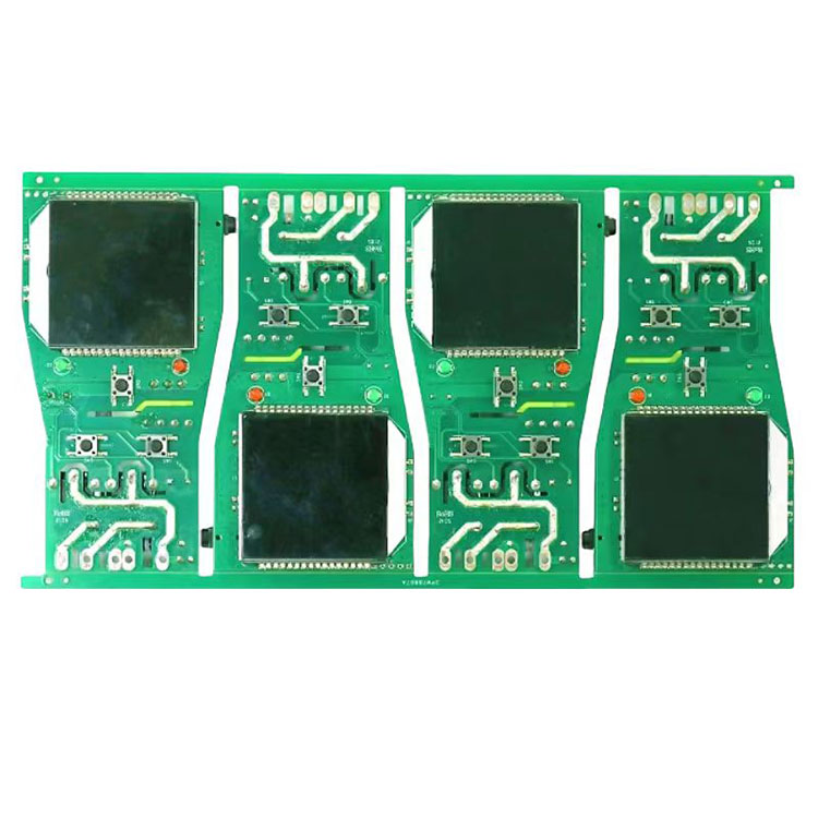
China 9 Layers PCB Board is an electronic board featuring ten layers of conductive material for signal routing. This 9 Layers PCB Board structure allows for complex circuit designs, accommodating a denser arrangement of electronic components. You use 10-layer printed circuit boards in applications that need proper electromagnetic conductivity. 9 Layers PCB Board free sample.
The standard stack-up of a 9 Layers PCB Board is a well-thought-out arrangement that balances signal integrity, power distribution, and grounding needs. This cheap 9 Layers PCB Board typically alternates between signal layers and power/ground layers, ensuring efficient circuit operation and minimizing issues like noise and interference.The typical configuration of a 9 Layers PCB Board includes multiple signal layers interspersed with ground and power layers.
Basic information:
Item: 9 Layers PCB Board
Layer Counts:9 Layers
Material: FR-4,Cu base,High TG FR-4,PTFE,Rogers,TEFLON etc.
Board thickness: 0.20mm-8.00mm
Maximum Size: 600mmX1200mm
Board Outline Tolerance: +0.10mm
Thickness Tolerance(t≥0.8mm): ±8%
Thickness Tolerance(t<0.8mm): ±10%
Insulation Layer Thickness: 0.075mm--5.00mm
Minimum Line:0.075mm
Minimum Space:0.075mm
Out Layer Copper Thickness: 18um--350um
Inner Layer Copper Thickness: 17um--175um
Drilling Hole(Mechanical): 0.15mm--6.35mm
Finish Hole(Mechanical): 0.10mm-6.30mm
Impedance control Tolerance:±10%
Surface finish/treatment: HASL,ENIG,Chem,Tin,Flash Gold, OSP, Gold Finger
Designing 9 Layers PCB Board, here are key points to consider:
Thickness of FR-4 Laminates: For PCBs with more than 6-8 layers, thinner FR-4 laminates, typically between 0.8 and 1.2 mm, are recommended over the standard 1.6 mm. This helps manage the board's overall thickness for fitting into electronic devices.
Material for High Frequencies: For higher frequency applications, materials with a low dielectric constant (Dk), different from standard FR-4, should be used. These materials improve signal integrity at high frequencies.
Glass Transition Temperature (Tg): The Tg should be over 170°C, especially for lead-free soldering and high-reliability applications. This ensures the material withstands high temperatures without degrading.
Glass Weave Styles: Using tight weave glass styles in laminates ensures more uniform dielectric properties, which is important for consistent electrical performance, particularly in high-speed applications.