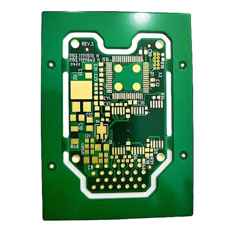
Blind Buried Hole PCB refers to the holes used to connect different levels of internal lines in multi-layer circuit boards. We are China's Blind Buried Hole PCB manufacturer. The plate does not penetrate the hole of the entire plate. The blind hole plays an important role in increasing the line density, reducing the plate size and improving the circuit performance. Blind Buried Hole PCB means that in the multi-layer circuit board, the aperture of the blind hole is welded inside the electrical connection to achieve the circuit connection inside the multi-layer circuit board.
Blind Buried Hole PCB and buried vias are a type of hole technology that connects inner layer wiring with top layer wiring using special processing methods. China Blind Buried Hole PCB used high-density wiring, improving the performance and reliability of the circuit board. Blind vias connect inner layer wiring to top layer wiring, while buried vias only connect inner layer wiring. Quality Blind Buried Hole PCB process is an important PCB processing technology, in order to achieve high density and high reliability in circuit board design, blind hole process is widely used Advancede Blind Buried Hole PCB.
Basic information:
Item name: Blind Buried Hole PCB
Base Material: Aluminum
Insulation Materials: Metal Composite Materials
Surface Finishing OSP, Immersion Gold, Immersion Tin, Immersion AG
Controlling Range: -40c~125c
Surface Finished: HASL, Gold Finger, OSP, Enig, Peelable Mask
Min. Line Width: 4mil
Specification: FR 4, 0.8mm, 1 Layer, 1OZ Copper Thickness
Max Production Size: 600*800mm
Blind Buried Hole PCB Features:
1. High-Density Design: PCB blind and buried hole boards use advanced technology to pack in more wiring, saving space and making electronic devices smaller.
2. Stable Signal Transmission: The blind and buried hole technology ensures that signals can travel between different layers without interference or crosstalk, keeping the circuit board stable and reliable. 3. Stronger Circuit Boards: The buried hole structure of the blind and buried hole board enhances the mechanical strength of the circuit board, making it more resistant to vibrations and distortion, increasing the durability of electronic devices.
4. Improved Circuit Performance: By using blind and buried hole technology, we can connect multiple layers of circuit boards for better signal transmission and power supply, boosting overall performance to meet the demands of complex electronic devices.