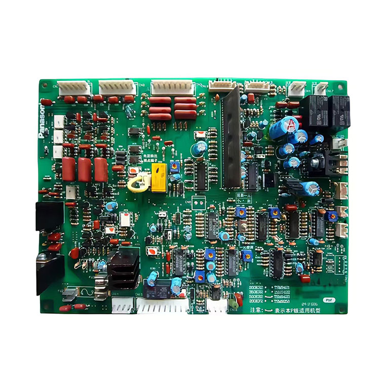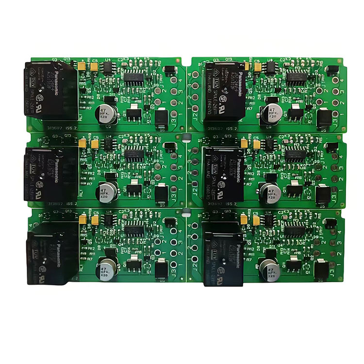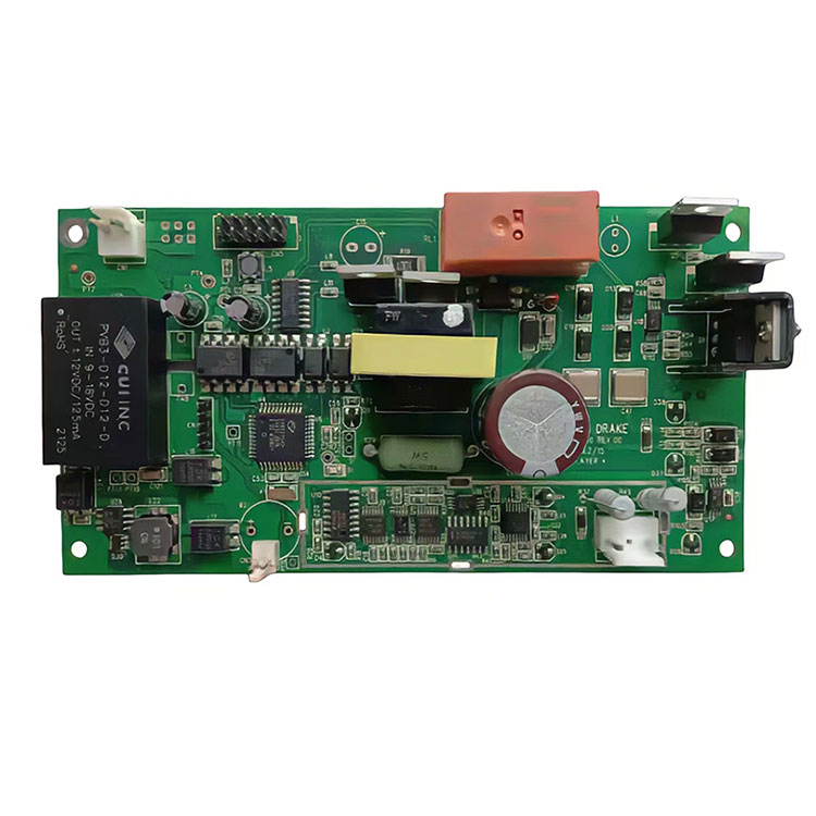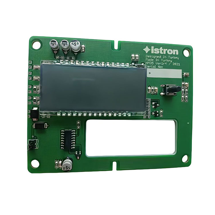
Wholesale Cross Blind Buried Hole PCB is a type of hole that connects the inner layers of a PCB to the outer layers, but it doesn't go all the way through the board. On the other hand, a buried via only connects the inner layers and isn't visible from the surface.Newest Cross Blind Buried Hole PCB .As portable products get smaller and more densely packed, designing PCBs has become tougher, with higher demands on production processes. For most portable products using BGA packages with 0.65mm pitch or less, we use blind and buried via design techniques.
Blind Via Hole connects the outer layer of a Cross Blind Buried Hole PCB to an inner layer through a plated hole, while Buried Hole connects internal circuit layers without reaching the outer layer. Cross Blind Buried Hole PCB factory. The Buried Hole process is more labor-intensive and expensive, but it's used for high-density circuit boards to maximize space.
Basic information:
Item name: Cross Blind Buried Hole PCB
Surface Finish: HASL Lf
Character: for Lighting
Transport Package: Vacuum Packing
Solder Mask Black
Base Material: Alu
Copper Thickness: 35um
Specification: 52mm*52mm
Cross Blind Buried Hole PCB Features:
1. Single, Double side & Multi-layer PCB.
2. Buried/Blind Vias, Via in Pad, Counter Sink Hole, Screw Hole(Counterbore), Press-fit, Half Hole.
3. HASL lead-free, Immersion Gold/ Silver/Tin, OSP, Gold plating/finger, Peelable mask,
4. Printed Circuit Boards adhere to IPC Class 2 & 3 international PCB standard.
5. Quantities range from prototype to medium&big batch production.
6.100% E-Test.


