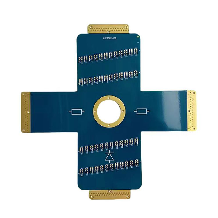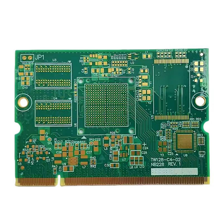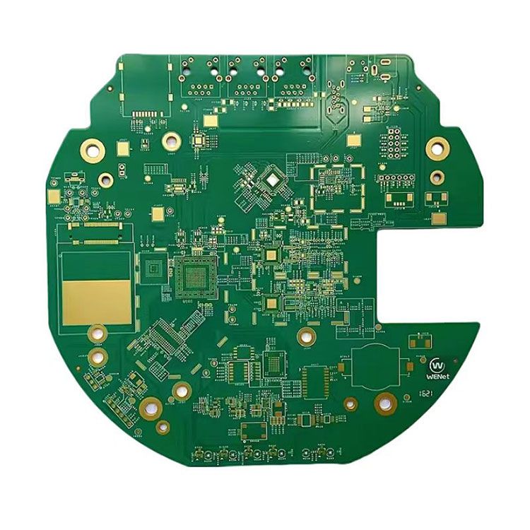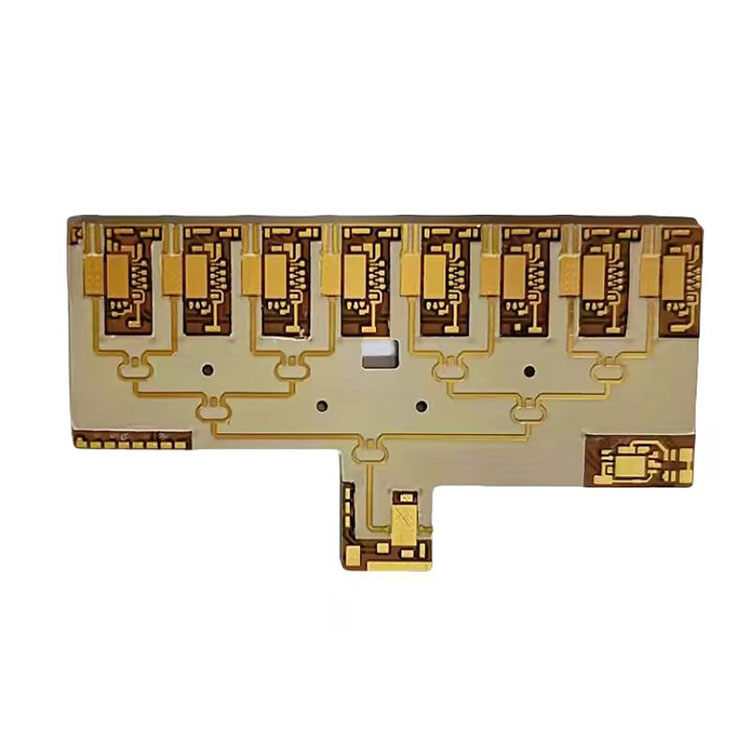
Customized Impedance Control PCB trace will be determined by its inductive and capacitive inductance, resistance, and conductance. Impedance Control PCB price refers to controlling the impedance of the wiring, which is also known as controlled impedance. Controlled impedance is the characteristic impedance of a transmission line formed by the Impedance Control PCB routing and its related reference planes. When high-frequency signals propagate on PCB transmission lines, they are correlated. Controlled impedance is crucial for solving signal integrity issues, which involve undistorted propagation of signals.
Impedance Control PCB in printed circuit boards involves the regulation of resistance exerted by signal traces. It is determined by characteristic China Impedance Control PCB factory, such as trace width and copper thickness. This article discusses Impedance Control PCB and the essentials of its execution in PCB manufacturing.
Basic information:
Name: Impedance Control PCB
Model Number: Multilayer PCB 57
Type: Multilayer PCB
Copper Thickness: 1 oz
Supplier Type: OEM
Max Layer Count: 48L
PCB Thickness: 0.2-6.5mm
Finished Size: 24.5*47inch
Max Base Copper Weight: 12OZ
Min Trace/Spacing: 2/2mil
Max PCB Aspect Ratio 20:1
Min BGA Pitch: 0.35mm
Min Impedance Tolerance: ±8%
Why Impedance Control PCB?
Usually, you need to control the impedance of PCBs used for high-speed digital applications, such as RF communication, telecommunications, calculations using signal frequencies above 100MHz, high-speed signal processing, and high-quality analog videos (such as DDR, HDMI, Gigabit Ethernet), ETC.
At high frequencies, the signal routing on the PCB is like a transmission line, with impedance at every point on the signal routing trajectory. If the impedance changes from one point to the next, there will be a signal reflection, and its amplitude will depend on the difference between the two impedances. The greater the difference, the greater the reflection. This reflection will propagate in the opposite direction of the signal, which means that the reflected signal will be superimposed on the main signal, resulting in distortion of the original signal.


