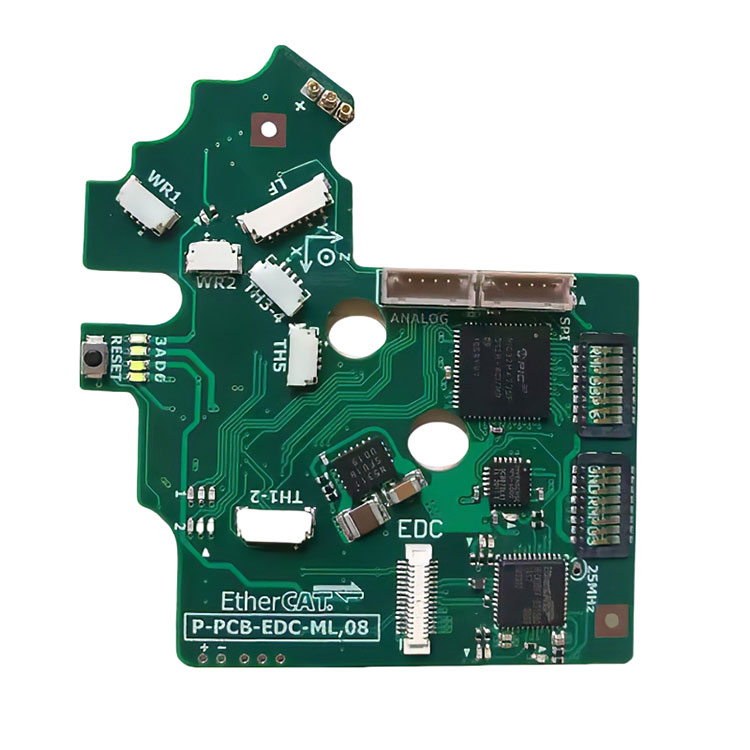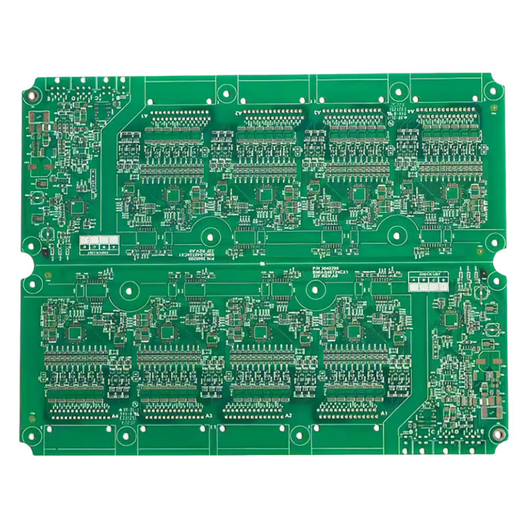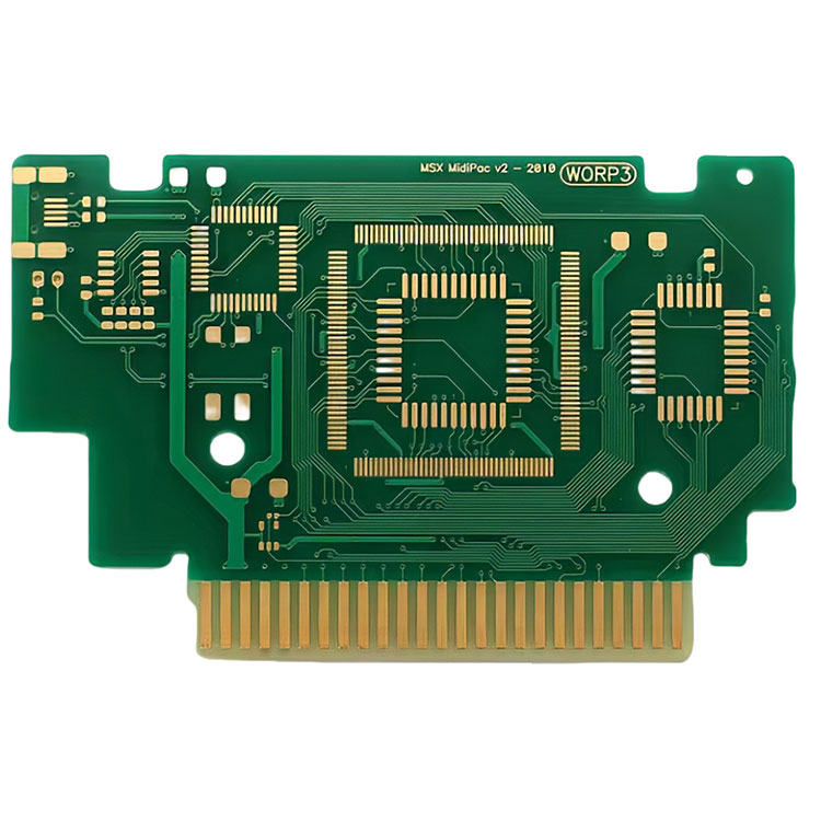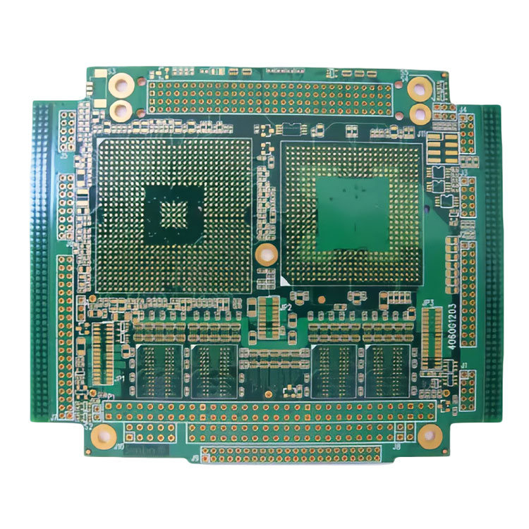
Let's examine the china 10 Layers Of HDI PCB. HDI (High Density Interconnector) is a type of circuit board produced using Microvia technology. The 10 Layers Of HDI PCB configuration indicates that there are 10 layers of interconnected circuits within the board, with each layer being linked through microholes. This customized 10 Layers Of HDI PCB is characterized by its compact size, lightweight construction, and high-speed signal transmission capabilities.
The primary characteristic of the 10 Layers Of HDI PCB blind buried hole board is its high density and precision. As an emerging technology in circuit board manufacturing,buy 10 Layers Of HDI PCB blind buried hole board is driving technological innovation in the electronic manufacturing industry with its exceptional performance and broad application. Wholesale 10 Layers Of HDI PCB market.
Basic information:
Item name: 10 Layers Of HDI PCB
Copper Thickness:0.5-3oz
Supplier Type:circuit board assembly Manufacturer
Layer:1-16
regular Board thickness:0.8/1.0/1.2/1.5/1.6/2.0mm
Assembly Type:FR4, FPC, Rigid-flex PCB, Metal base PCB
Assembly Specification:Min size L50*W50mm; Max size: L510*460mm
Assembly thickness Min thickness: 0.2mm; Max thickness: 3.0mm
Minimum device accuracy:+/-0.04mm
Minimum footprint distance:0.3mm
Capacity:SMT 500W point/day;THT 30W point/day
Certificate:ROHS/ISO9001
Utilizing a 10 Layers Of HDI PCB offers advantages, such as:
Higher circuit density
Enhanced signal integrity
Improved thermal regulation
Better EMC performance
Decreased size and weight
Increased dependability
Simplified compliance, with design specifications
Lowered interference levels
Improved manufacturing oversight


