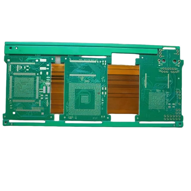


New Large Size HDI PCB are generally manufactured using the stack-up method, and the more times the layers are stacked, the higher the technical grade of the board. Large Size HDI PCB is made in china.These are conducive to the use of advanced assembly technologies, and their electrical performance and signal accuracy are higher than those of traditional PCBs. In addition, Large Size HDI PCB have better performance in improving radio frequency interference, electromagnetic interference, electrostatic discharge, heat conduction, etc. Hongxinda Cooperation offer cheap Large Size HDI PCB, inquiry is welcome.
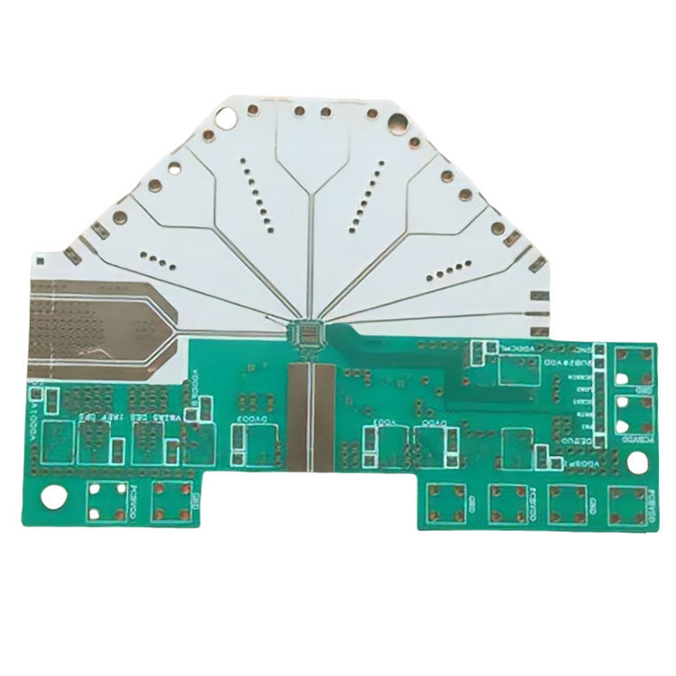
Large Size HDI PCB is a traditional dual panel as the core board, through continuous stacking layer by layer. This kind of circuit board made by continuous layering is also called Build-up Multilayer (BUM). Compared with traditional circuit boards, HDI circuit boards have the advantages of "light, thin, short and small". We offer customized Large Size HDI PCB .The electrical interconnection between the board layers is realized through the conductive through hole, buried hole and blind hole connection, its structure is different from the ordinary multi-layer circuit board, and a large number of micro-buried blind holes are used in HDI board.We provide Large Size HDI PCB free sample ,come and see if it's what you need.
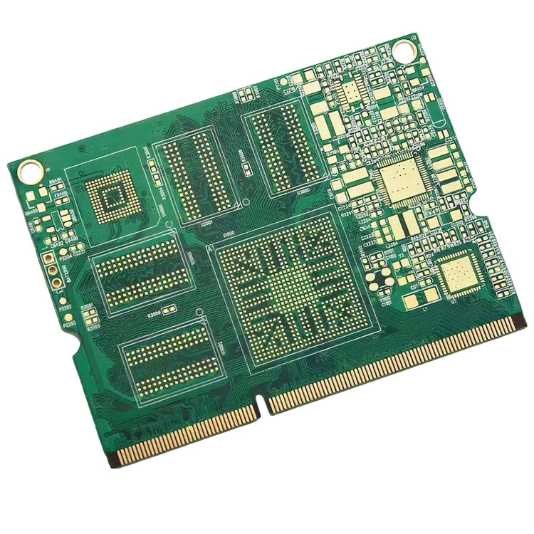
Item name: Large Size HDI PCB
Dielectric: FR-4
Application: Communication
Mechanical Rigid: Rigid
Base Material: Copper
Min.Hole Size: 0.1mm(4mil) for HDI/0.15mm(6mil)
Type:Rigid Circuit Board
Material:Fiberglass Epoxy
Processing Technology: Electrolytic Foil
Insulation Materials: Epoxy Resin
Surface Finishing: Immersion Silver,Tin,Gold/HASL Lead Free
1. The plate contains micro-pilot holes such as blind holes;
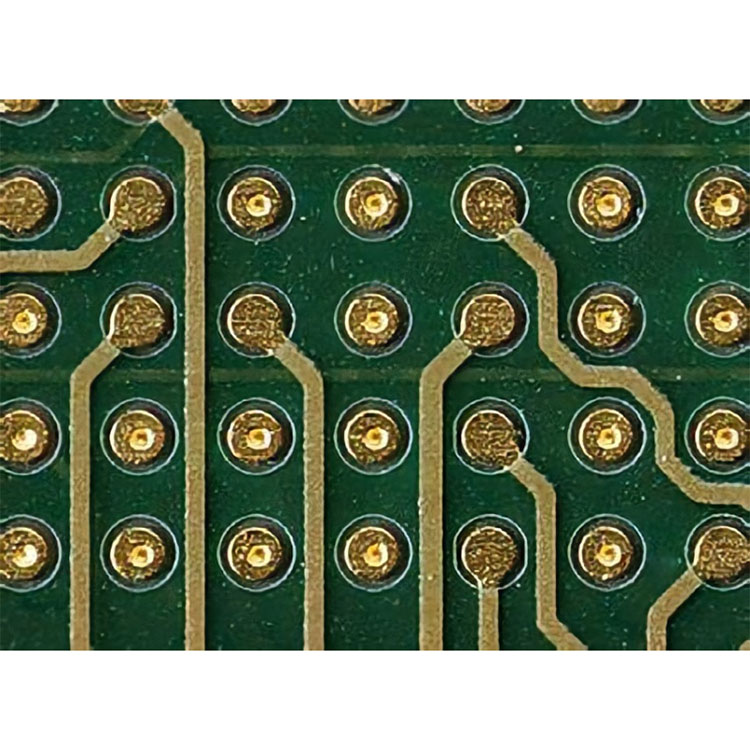
2. The aperture is less than 152.4um, and the hole ring is less than 254um;
3. Welding contact density greater than 50cm/ cm2;
4. Wiring density greater than 46 cm/cm2;
5. The width and distance of the line shall not exceed 76.2um.