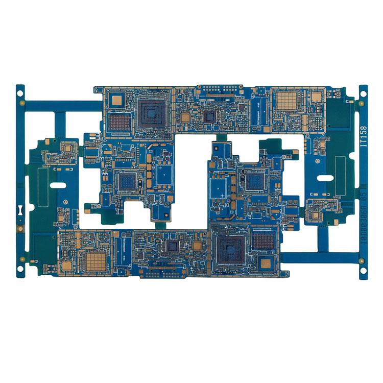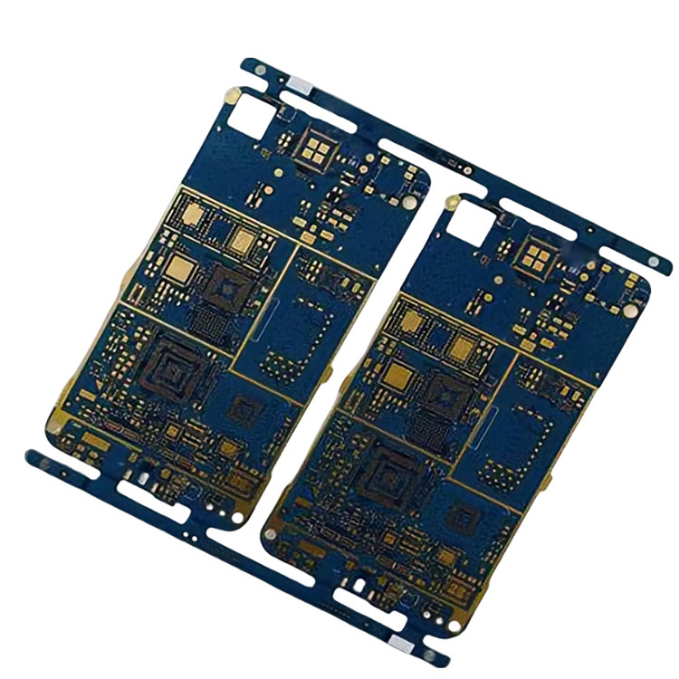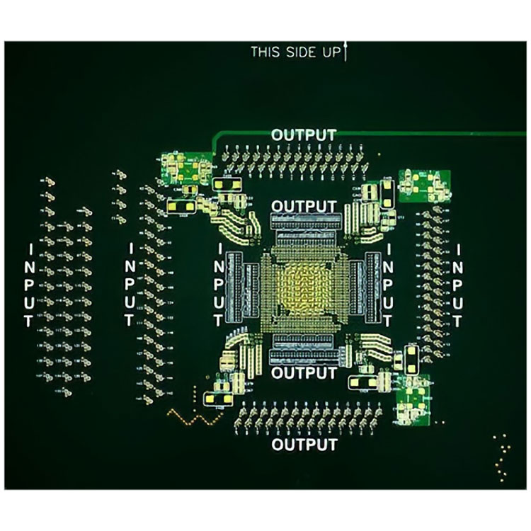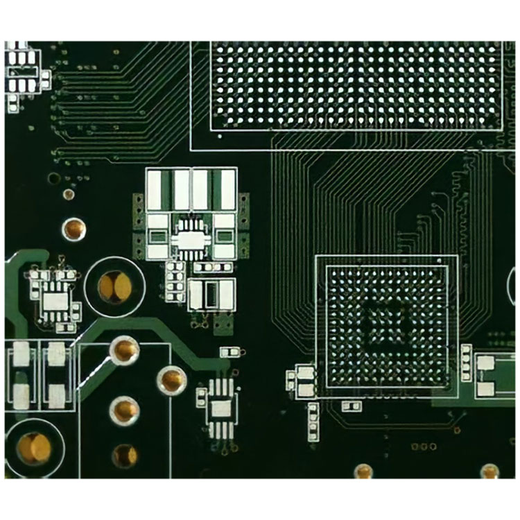
8-layers 3Step HDI PCB, one of the fastest growing technologies in PCBs. In an china 8-layers 3Step HDI PCB, each layer functions as an independent microstrip line, with the interconnection achieved through capacitive coupling between the microstrip lines. The impedance of each individual layer directly impacts the overall impedance of the advanced 8-layers 3Step HDI PCB.
In the realm of modern electronic devices, high quality 8-layers 3Step HDI PCB has emerged as a crucial design trend. Our company is china 8-layers 3Step HDI PCB supplier, particularly the widely utilized 8-layers 3Step HDI PCB (High Density Interconnector) in communication equipment, computers, medical devices and other fields due to its advantages in high frequency, low signal loss and excellent thermal performance.
Basic information:
Product name: 8-layers 3Step HDI PCB
Model: HDI PCB
Package: original
Minimum line width: 0.1mm
Minimum aperture: 0.1mm
pcb batch cycle: 6-7 days
Quality inspection: AOI, 100% E-test
Special process: resin plug hole
Reinforcing material: glass fiber cloth base
Maximum operating temperature: 125C
Level: Level A
8-layers 3Step HDI PCB after-sales:
Our company's service is not only limited to high efficiency and high quality, but more importantly, the deep understanding and accurate grasp of customer needs, so that you feel unparalleled intimate service.


