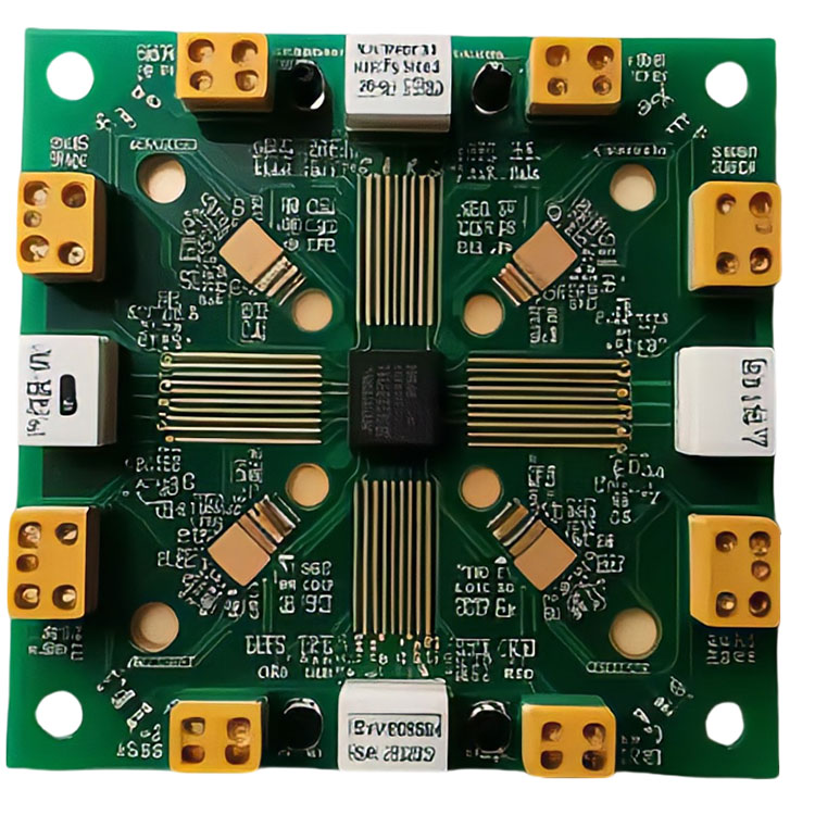
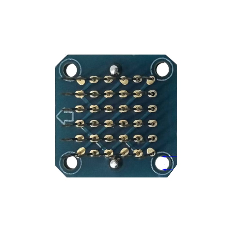
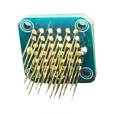


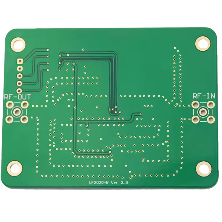
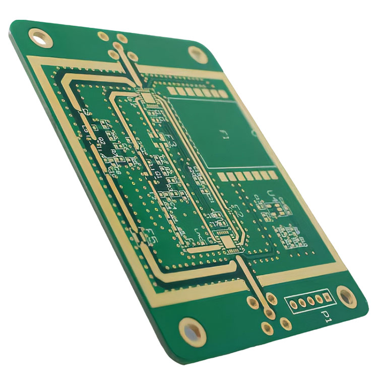
we are one excellent Multilayer Layers HDI PCB manufacturer in China. The Multilayer Layers HDI PCB aims to achieve a higher level of circuit integration by incorporating denser micro-holes and micro-traces on top of the traditional cheap Multilayer Layers HDI PCB, typically comprising multiple interconnected conductive layers through micro-vias to enable intricate circuit designs.
The HDI circuit board is a Multilayer Layers HDI PCB produced using the stacking method and micro-blind hole technology. In other words, high quality Multilayer Layers HDI PCB with or without electroplated through holes (PTH) is initially obtained following traditional practices, after which the two outer layers are constructed with thin lines and micro-blind holes. Our company's technological innovations have given it a competitive edge in the market.Hongxinda offer cheap Multilayer Layers HDI PCB,hope to receive your inquire about this item.
Basic information:
Item name: Multilayer Layers HDI PCB
Min. Hole Size:0.1mm(4mil)for HDI / 0.15mm(6mil)
Min. Line Width:0.075mm/0.075mm(3mil/3mil)
Min. Line Spacing:0.003''
Surface Finishing:HASL/OSP/Ag/ENIG/ENEPIG/Immersion silver/Tin
Layer No. :2-32 Layers
PCB Test:Flying probe and AOI (Default)/Fixture Test
Base, Cover film, Stiffeners thickness:0.5mil, 1.0mil, 2.0mil, 3.0mil, 4.0mil, 5.0mil, 6.0mil,0.10um
BGA Ball Pitch:1mm ~ 3mm(4mil ~ 12mil)
PCB Assembly Method:SMT, Through-hole, Mixed, BGA
PCB Assembly Test:Visual Inspection (default), AOI, FCT, X-RAY
Hi-TG FR4 Material:Tg-130 Tg-140 Tg-160 Tg-170
Multilayer Layers HDI PCB four technical conditions:
1. The aperture of the through hole: ≤100μm; Connecting disc diameter (hole ring diameter) : ≤250μm;
2. Through hole density: ≥ 60 holes/square inch (930,000 holes/m2);
3. Wire width/spacing (L/S) : ≤100μm/100μm;
4. Wiring density: ≥ 117 inches/square inch (46cm/ cm2).